Digital circuit design entails ideation, creation, and revision. Study PCB design and the circuit layout system.
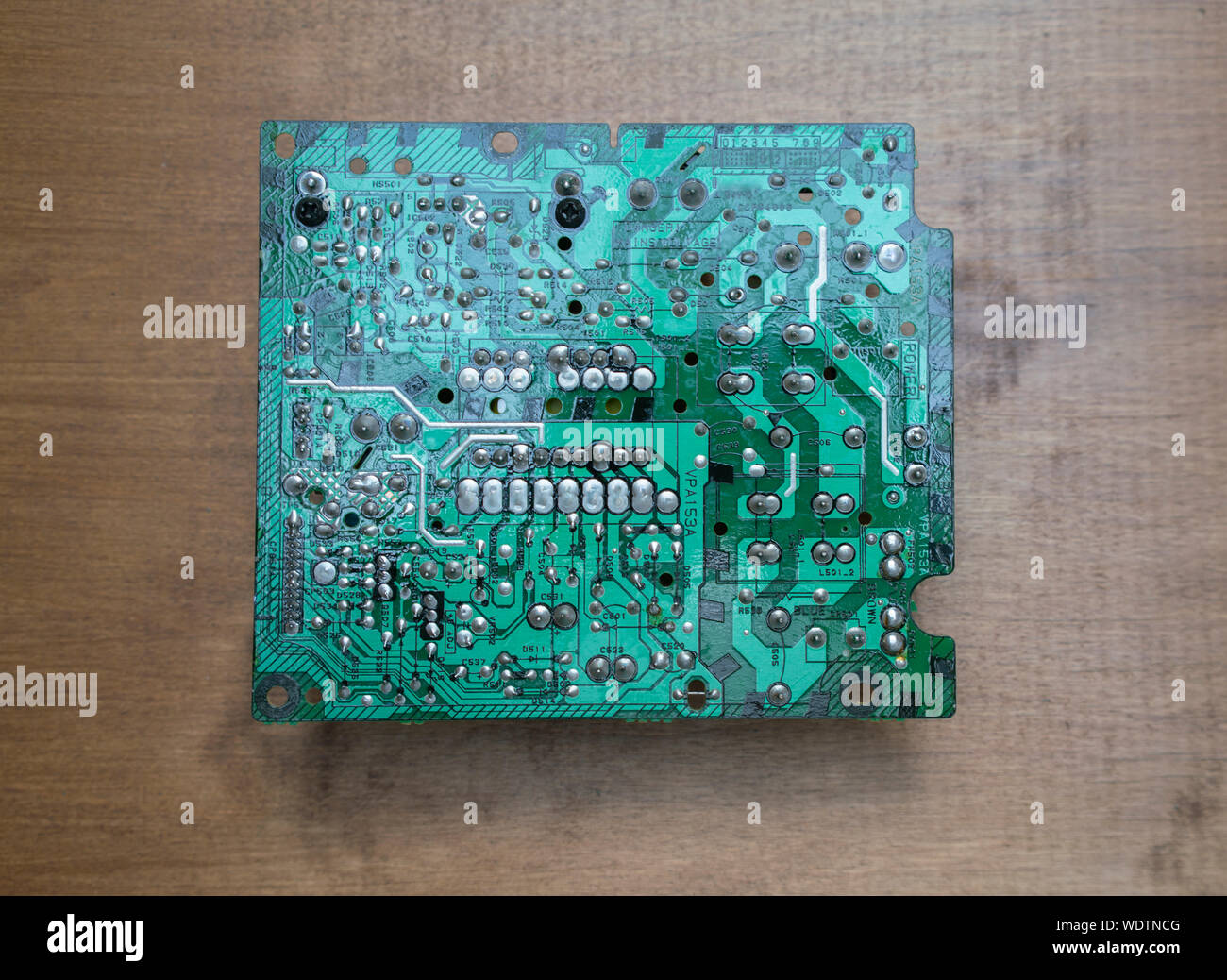
(PCBs) are in each piece of contemporary electronic device, which is why it’s critical to recognize what, exactly, a circuit board consists of and how designers can put in force it into so many applications.
Designing a digital circuit starts at the breadboard (protoboard). The bedboard is a skinny, plastic, rectangular production base to which digital components are soldered. The soldered connections aren’t everlasting and can be removed and relocated over and over within reason.
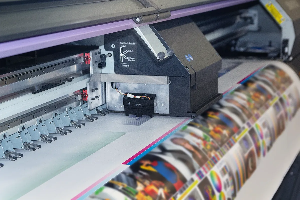
The development of a breadboard finally turns it into what’s referred to as a PCB, frequently used in computations, signal amplification, and information transfer.
The interconnections on a PCB join the soldered components. The rate flows from the tremendous terminal throughout the interconnection loops to the negative terminal.
The Basics of Digital Circuit Layout
Included Circuits (ICs) have Hugely Improved
Metal-oxide-semiconductor field-effect transistors (MOSFETs). There are 3 commonplace circuit designs: analog, digital, and blended-signal.
Analog Circuit Layout
Analog circuit designs typically encompass diodes, transistors, transformers, operational amplifiers, and other passive components. Those circuits carry out complex record analyses, filtering, and amplification.
Virtual Circuit Layout
Virtual circuit design features on discrete values (zeros and ones). Those are commonly a part of the entire PCB design.
Combined Circuit Design
In lots of contemporary packages, PCB designers do not often use only analog or virtual circuit layouts. Virtual and analog circuits are separated to reduce noise and enhance overall performance.
Microcontroller
Microcontrollers include digital circuits that you could program to carry out a range of instructions.
Discipline Programmable Gate Arrays (FPGA)
FPGAs are digital circuit forums that you may at once configure on a hardware stage in place of the usage of a hard and fast of instructions. FPGAs are high-quality devices used for high-performance systems, which include aerospace applications.
Schematic Circuit Diagrams
A schematic circuit diagram represents additives and interconnections in a PCB layout. Those commonly use standardized symbols and are dimensional and are often utilized in construction and electrical preservation.
The Circuit Design Procedure
The circuit design procedure is full-size — it includes ideation, trying out, prototyping, revising, and retesting. Circuit design goes through numerous iterations, like the writing method, before reaching a final product. Each process starts with the definition preparation of the idea.
Outlining
Outlining is one of the most critical components of circuit design. Outlining is when the dressmaker prepares the structure of the PCB. Distinctiveness additives, like incorporatedcircuitsts are selected during this stage.
Schematic Drawing Once entire, the design is translated onto a schematic in which additives are connected to achieve circuit capability. This manner generally involves many components, modules, and subcircuits.
PCB format
On this degree, the PCB drawing is now a PCB format initiated via shifting additives into the schematic. The schematic is checked for mistakes, and the revision procedure begins. It’s not unusual for additives to rearrange to resolve schematic mistakes or layout rule violations.
Prototyping
Prototyping involves fabricating the PCB in small volumes to ensure functionality. You should report design mistakes and the timetable for revision in the course of the next round of format changes.
Thing Placement
Depending on the manufactured prototype, components are positioned on the PCB. For example, analog components have to have adequate clearance from their high-speed virtual counterparts. Thing placement has to alleviate future servicing and troubleshooting. In a manner, this is designed for accessibility. It needs to be much less complex to provide the PCB after several factor placement revisions.
Electromagnetic Interference (EMI) Check
EMI should be checked at a growing fee. This is because electronics are getting smaller, faster, and wireless. The fine technique to EMI issues is to well separate floor planes to house high-velocity signals.
Power Delivery Network
Energy modules are the lifeblood of the PCB. Therefore, a bad electricity module may want to without difficulty sink an otherwise ideal PCB design. A very good energy shipping network ensures minimum strength loss.
Autodesk Fusion 360 offers you get right of entry to to comprehensive electronics and PCB layout tools in a software solution. Get started today with a 30-day free trial.